14. 8. 2019 15:00 - 16:00 SELČ online webinář
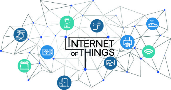 The Internet of Things (IoT) is not a new topic to many; however, the rapidly changing wireless technology used in IoT devices may be. Billions of new IoT devices will be coming online in the next few years, and 5G technologies will be the foundation for the design of devices like smartphones, tablets, laptops, and wearables. This presents new design challenges: What do I need to use for board materials? What type of antenna do I need to use? What are the requirements for PCB design? All these and many more are concerns you will need to start investigating and finding solutions to in order to successfully design your first- or next-generation wireless device.
You may be thinking PCB materials will be your biggest concern. Depending on the device you’re creating and communication protocol you will be using, the carrier frequency you'll need to use could range from 6 GHz up to 80 GHz. This means that how you define your board stack-up, place components, route traces, and where you place vias will pose as much of a challenge as choosing materials if you want your design to work properly.
What You Will Learn:
- RF design practices for first-pass success
- Tools required to make the design process less painful
- Modern layout techniques for 5G wireless
Na tento online seminář se můžete registrovat také přímo ze stránek programu PADS.